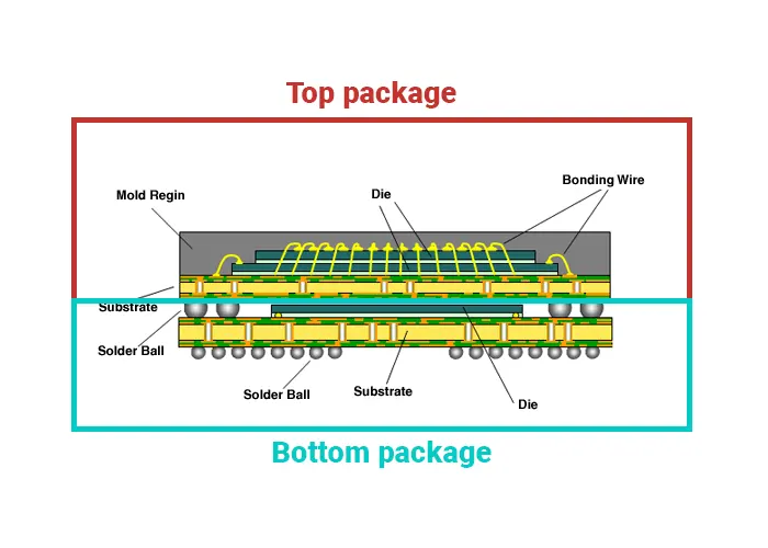
PoP stands for Package-on-Package Assembly which is a configuration where two packaged integrated circuits are placed directly on top of each other (can also be known as stacked packages)
Interconnects are between the top package and the bottom package and the bottom and the PCB:
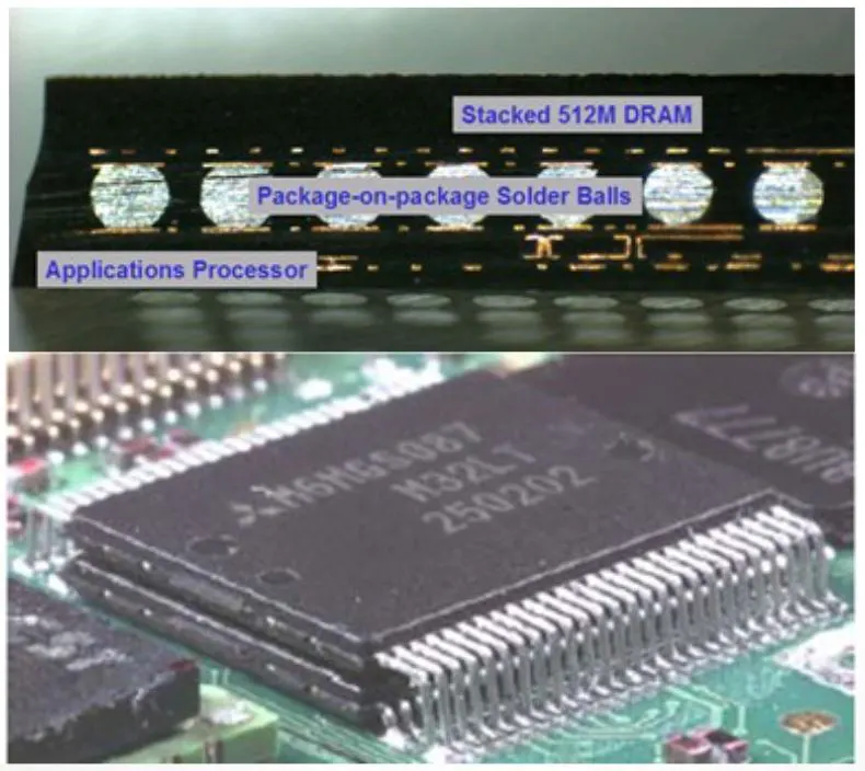
Top package traditionally contains multiple or stacked die
Bottom package traditionally contains smaller/ thinner die
Bottom Package
Has land pads on the top perimeter to allow for top PoP attach
Molded using a special process to keep the perimeter clear
Requires thin die and mold cap to allow for top package clearance
Top Package
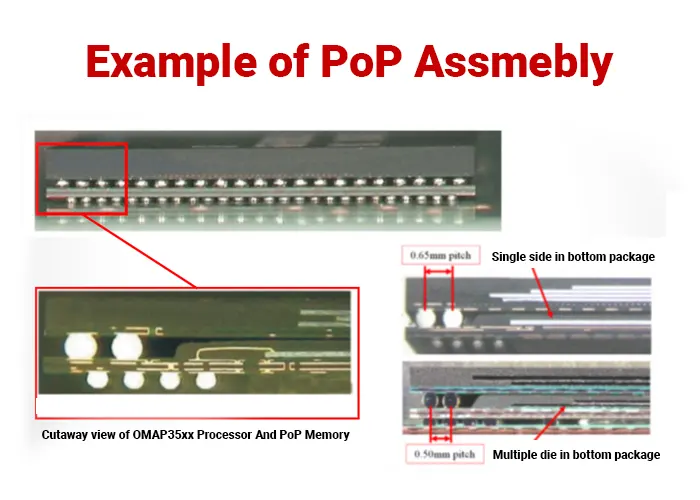
Based on conventional stacked die BGA but with larger ball size and thinner mold body
Ball pitch and size are constrained by the need to clear the bottom package
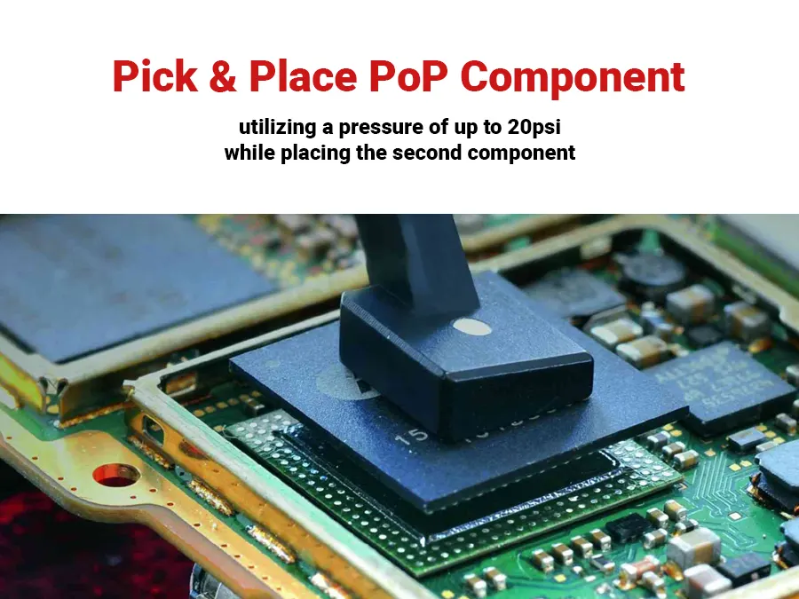
The package must be capable of being placed on the printed circuit board (PCB) and reflowed simultaneously to each other and to the board.
Why PoP? The benefits of Package-on-Package Assembly?
The benefits of PoP are well known. They include:
Less board real estate
Better performance (shorter communication paths between the micro and memory)
Lower junction temperatures (at least compared to stacked die)
Greater control over the supply chain (opportunity to upgrade memory and multiple vendors)
Easier to debug and perform F/A (again, compared to stacked die or multi-chip module or system in package)
Ownership is clearly defined: the bottom package is the logic manufacturer, the top package is the memory manufacturer, and the two connections (at least for one-pass) are the OEM
Where will PoP be used?
Dominant use
Integration of digital logic device in a bottom package with combination memory devices (i.e. DRAM and flash) in the top package